This Samsung S23 Ultra came to us with a single complaint: it wouldn't charge. However, what we discovered inside turned it into one of our most technically complex cases, with a solution that may surprise you.

What You'll Need for This Repair
- REFOX RS30 ESD Repair Heat Mat — Anti-static heating pad for safe adhesive softening
- REFOX RS70 PryPal Blade Kit — Precision blades for separating back covers without damage
- REFOX RS75 Universal Knife Handle Set — Dual-head precision tool for disconnecting flex cables
- USB-C test board
- Digital multimeter
- REFOX Bitmap (schematic reference)
- Precision grinding pen
- Kapton tape (heat-resistant insulating tape)
- 0.1mm enameled wire (ultra-thin insulated copper wire for micro-soldering)
- Solder flux and medium-temperature solder paste
- UV-cure solder mask (green oil)
- UV lamp
- High-temperature tape
Step 1: Initial Diagnosis — Connect the USB-C Test Board

The first step in any charging fault is to avoid assumptions. We connected a USB-C test board — a diagnostic tool that lets you probe individual electrical traces on the charging circuit without fully disassembling the phone. This saves time and prevents unnecessary teardown.
We ran diode readings across all the major charging-related traces.
Most traces came back normal. But when we probed the VBUS trace, we got a zero reading — a confirmed short.

Step 2: Teardown — Getting to the Motherboard
Soften the Adhesive
Place the phone on the REFOX RS30 ESD Repair Heat Mat set to 90°C for 1–2 minutes.

Remove the Back Cover
Use the REFOX RS70 PryPal Blade Kit to carefully slide between the frame and back cover and separate them. Work slowly around the perimeter — don't rush this step.

On the S23 Ultra, the back cover and wireless charging coil assembly are separate components. This is good news: you can lift the back cover cleanly without disturbing the wireless charging hardware.
Protect the Cameras
Before going any further, place a protective cover over the rear camera array. The S23 Ultra's camera lenses and sensors are extremely vulnerable to micro-scratches from tools or debris during disassembly. This is a step many technicians skip — and regret.

Disconnect Flex Cables and Remove the Motherboard
Use the REFOX RS75 Universal Knife Handle Set to carefully disconnect all flex cables.

Once all cables are disconnected, the motherboard can be carefully lifted out.
Step 3: Confirm the Fault on the Motherboard
With the motherboard out, we referenced the REFOX Bitmap — our schematic reference that maps every trace and component location on the board — to locate the VBUS terminal on the FPC connector.

We probed the VBUS terminal. The reading was still abnormal — confirming the short was on the board itself, not in the charging port. The port was fine. The problem was deeper.
Next question: had the output circuit survived?
Step 4: Check the Output Circuit
The output circuit — the side of the charging path that delivers power to the battery and internals — sits underneath a metal shield on the back of the motherboard.

Why We Used a Grinding Pen Instead of a Heat Gun
Normally, technicians use a heat gun to remove shields. Here, we chose a precision grinding pen instead.
We probed the output circuit — and got normal readings. The output side was intact. The fault was fully isolated to the input trace.
Step 5: Rule Out the Capacitor
A small capacitor near the VBUS trace could theoretically be causing interference. We isolated it, desoldered it, and re-tested the input trace.

Still shorted.
With the capacitor eliminated as a variable, the conclusion was unavoidable: the fault was inside the motherboard's internal copper layers — not on the surface, not in any component. The trace itself, buried between laminated layers of the board, was shorted internally.
Step 6: The Hard Decision — Split the Board or Find Another Way?
Standard procedure for an internal trace fault is to split the motherboard — physically separate its bonded layers to access and repair the damaged trace. On older devices, this is manageable. On Samsung's S20 series and beyond, it's a different story.

Here's the problem:
- Samsung uses large amounts of high-temperature solder paste in the middle bonding layer
- Melting it requires sustained, prolonged heat — far longer than a typical reflow
- That sustained heat causes CPU and UFS chip pseudo-soldering — joints that look intact but have actually weakened at a microscopic level
Once the CPU or UFS is disturbed, the phone is classified as "heavily repaired" — and its resale value drops significantly. The risk-to-reward ratio of a board split on this device was simply too high.
So: was there another way?
Step 7: The Jumper Wire Solution
After a technical review, the REFOX team engineered a jumper wire bypass — routing power around the dead VBUS trace entirely, without touching the internal layers.

The logic: since the VBUS input trace is dead, we run a new wire directly from the flex cable connector (where power enters from the charging port) to the output inductor (where power exits toward the rest of the board), bypassing the broken section entirely.
Risks of the Jumper Wire Approach
We informed the owner of all risks. He understood and agreed to proceed.
Step 8: Performing the Jumper Wire Repair
Remove the Bottom Speaker
Unscrew and remove the bottom speaker module to gain clear access to the work area on the motherboard.
Prepare the Output Inductor

Apply a controlled amount of flux to the output inductor.
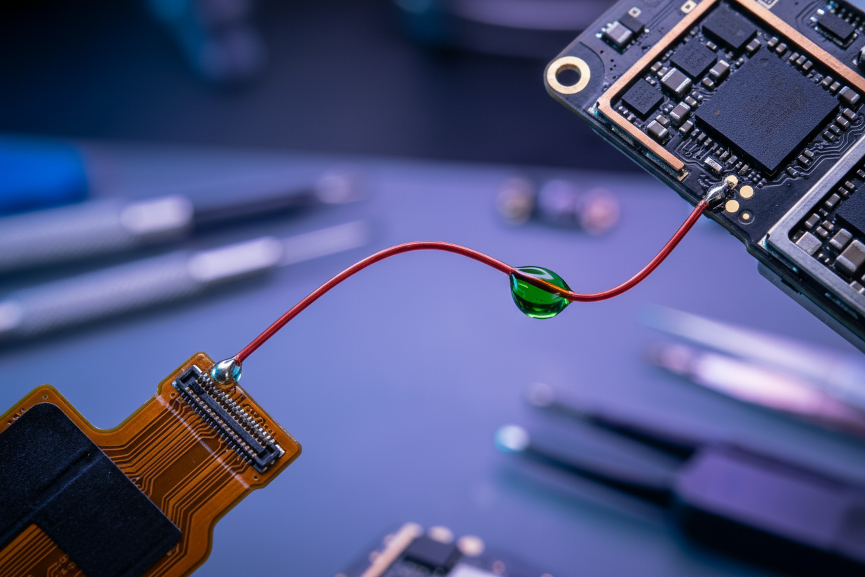
Solder the Wire to the Inductor
Using 0.1mm enameled wire, carefully solder one end to the output inductor. This wire is approximately the width of a human hair — it demands a steady hand, proper magnification, and a fine-tipped soldering iron.

Clean and Insulate
- Clean the solder joint with a flux-cleaning sponge
- Apply UV solder mask (green oil) over the joint
- Cure with a UV lamp
This "insulation armor" locks the wire mechanically and prevents it from vibrating loose under normal use.
Prepare the Flex Cable Connector End

- Gently scrape the coating off the target pad on the flex cable connector to expose bare copper
- Apply medium-temperature solder paste
- Add flux and solder the other end of the wire to this pad
- Clean thoroughly with IPA or flux cleaner
- Apply UV mask for insulation and cure under UV lamp
Verify with Multimeter

Probe the VBUS trace again. The readings should now be back to normal — and they were. The bypass was confirmed live.
Resolder the Capacitor
Solder the small capacitor back to its original position. Don't skip this — it plays a role in filtering the charging circuit.
Isolate the Original Faulty Input Pins
Apply a piece of high-temperature tape over the original VBUS input pins on the connector. This fully isolates the dead trace and ensures it cannot interfere with the new bypass path.
Step 9: Reassembly and Testing

Snap the flex cable connector back on — it should seat firmly with a clean click. Reassemble the motherboard and reconnect all flex cables in the reverse order of removal. Take your time here; a misaligned connector can introduce new faults.
Results:
- ✅ Charging function: restored and working normally
- ✅ OTG function (using USB-C as a power output to other devices): intact and working
Board Split vs. Jumper Wire: Which Is Right?
| Board Split | Jumper Wire | |
|---|---|---|
| Repair quality | Permanent, factory-like | Functional, non-standard |
| Risk to CPU/UFS | High | None |
| Resale value impact | Significant | Moderate |
| Skill required | Extreme | High |
| Best for | Warranty / insurance repairs | Customer-agreed value repairs |
Conclusion
What looked like a simple charging fault turned out to be a lesson in one of the most important skills in professional repair: knowing when not to follow the textbook.
The standard answer — split the board — exists for good reason. It's the cleanest, most permanent fix. But on a Samsung S23 Ultra, the risks of that procedure are real and significant. A damaged CPU or UFS chip doesn't just cost money; it can mean permanent data loss for the customer. That's not a trade-off to make lightly.
The jumper wire solution we used here isn't a shortcut. It required precise diagnosis, careful schematic reading, steady micro-soldering, and proper insulation. It also required honesty — fully informing the customer of the trade-offs and getting their informed consent before proceeding.
At REFOX Lab, every repair decision starts with one question: what outcome is genuinely best for the device and the owner? In this case, a 0.1mm wire and a steady hand gave this S23 Ultra a second life — with the CPU and UFS chip untouched, and the customer fully in the loop.
🛠️ Tips & Tricks from the REFOX Lab Bench
These are the hard-won insights from this repair — the kind of knowledge that only comes from doing the work. Whether you're a seasoned technician or learning board-level repair, keep these principles close.
What would you have done — full board split, or the jumper wire bypass? Drop your thoughts in the comments below, and watch the full repair on YouTube.
Deel:
Hoe los je de melding "Onbekend onderdeel" op het iPhone-scherm in iOS 26.1 op (gegarandeerde methode)?
Essential Repair Tools and Machines Every Professional Repair Shop Needs in 2026